BIPOLAR JUNCTION TRANSISTOR (BJT)
Transistors are very important component used as a switches and amplifiers. In almost all electronic equipment amplification is achieved by passing the signal from the low resistance to high resistance. Hence we call it as transistor. The transistor of two type’s
- Bipolar junction transistor
- Field effect transistor
Here we are going to see about bipolar junction transistor
Bipolar junction transistor
The BJT was invented in 1947 by john Bardeen and Walter Brattain and in 1951 William Shockley made modern version of the transistor BJT. This invention completely revolutionized in electronic industry and transistor much wide spread application in computer chips, communication satellite, calculator etc.
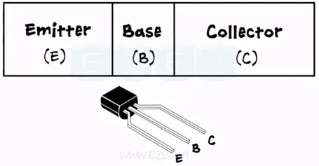
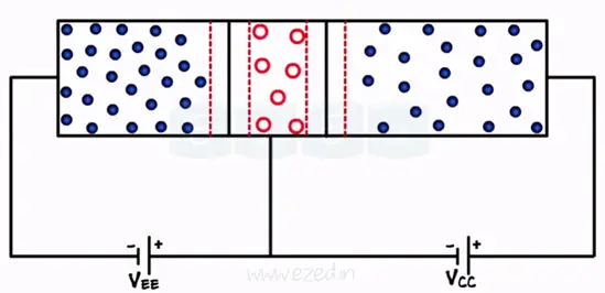
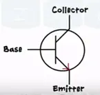
BJT is a silicon or germanium crystal containing three separate regions emitter (E), base (B), collector (C) thus obtaining three terminal devices.
 Current conduction in BJT is due to two types of charge carriers that is holes and electrons as it is called bipolar junction transistor.
BJT is classified into two types
- NPN transistor
- PNP transistor
Construction of Bipolar junction transistor
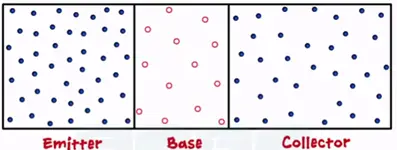
When we insert the P type semiconductor in between the N type semiconductor we get an NPN structure out of three region emitter is heavily doped with N type impurities. Base is very lightly doped with P type and doping concentration of N type impurities in the collector lies between base and emitter. Hence emitter and collector containing free electrons and base region has free holes as majority charge carriers.
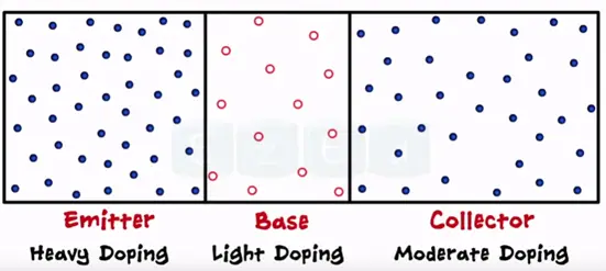
These three regions are not equal area emitter acts as source and collector as a destination of charge carriers. The collector occupies the highest area to collect maximum electrons next is emitter and base is lowest area.
When we insert the N type semiconductor in between the N type semiconductor we get PNP semiconductor. Doping concentration in PNP also remains the same with emitter heavily doped. Collector is moderately doped and base is very lightly doped. Areas are kept unequally again. In PNP emitter and collector has a hole whereas base contains free electrons of majority charge carriers.

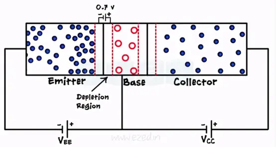
As we get two PN junctions as base to emitter junction and base to collector junction. We consider as a two diode for analogy to transistors.
Working of NPN transistor
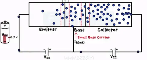
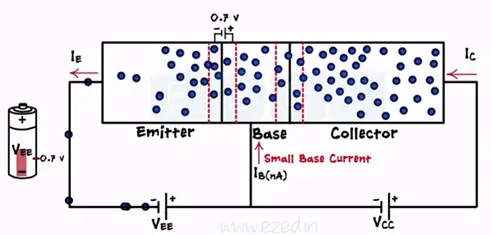
We connect two DC source such that base to emitter junction will be forward bias and collector to base junction will be revered biased. Source connected to the base to emitter junction is called as Vᴇᴇ and one collector to base is called Vᴄᴄ.
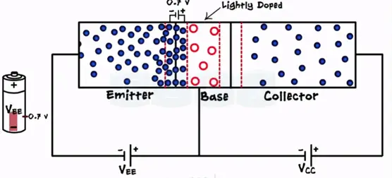
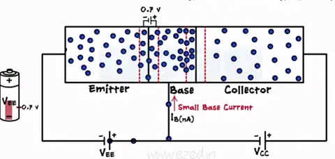
When we apply negative terminal to DC to the emitter electron from the emitter moves towards base being a PN junction forms the junction potential 0.6 V to 0.7V. electron reach the depletion region but can’t cross the depletion region. When we increase the Vee voltage in junction potential value the electron will successfully cross the depletion region and enter into the base. The base is lightly doped P type impurities contain very few holes as majority carriers. All the electrons cross over the junction only 5% electron recombine with holes and constitute the base current. which is very small in nano ampere range and remaining 95% of electrons continue towards motion towards the collector terminal as it move positive terminal base. These electrons along with the collector region towards the positive terminal of battery it will flow to the collector current collector to emitter. The expression for emitter current become Iᴇ=Iᴃ+I ᴄ
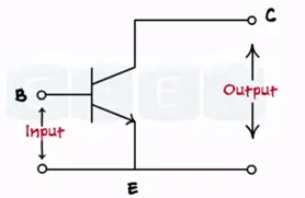
In NPN transistor flow of current in emitter terminal repeated by showing arrow heading towards the emitter as symbol of NPN transistor as shown.
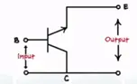
Working of PNP transistor
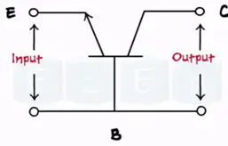
The working of PNP transistor is similar to working of NPN transistor. By applying input to getting output one of three terminals is always common terminals. Based on these concepts there are three basic configuration of BJT as common base (CB) common emitter (CE) and common collector (CC).
In common base configuration we apply input in between emitter and base and we measure output between collector and base. Thus the base acts as a common terminal for input and output. In CE configuration common acts as common terminal for this transistor used as an amplifier in CE configuration and in CC configuration collector acts as a common terminal.


