JFET Working Principle:
In Our Last Study we have seen the full functionality of BJT Bipolar Junction Transistor. From That You can come to know BJT is Current controlled device. The transistor operation can be completely controlled by the base current of the BJT. In BJT both minority and majority carriers are involved in the operation. On the other hand, a junction field effect transistor is a voltage controlled device, and FET operation is depending upon only the majority carriers. Also, both transistors are three terminal devices. However, FET is divided into two categories and they are JFET and MOSFET.
Coming to the construction of JFET, the p-type or n-type semiconductor placed in between two N-type or P-type semiconductor which forms like N-P-N or P-N-P. Here the middle portion has large channel. And the type of middle portion, it is divided into two categories One is N-channel JFET and another is P- Channel JFET. For The sake of understanding we are going to study about N-channel JFET.
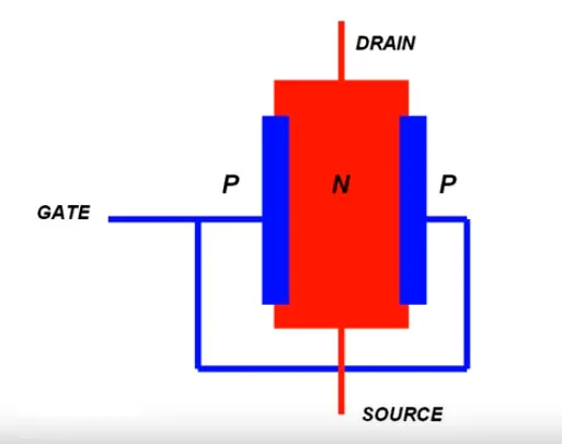
In N-channel JFET consists of three terminals such as GATE (G), Drain (D), and Source (S). The middle portion of N type semiconductor has two terminals such as drain and source. The metallic terminal connected to the layer surrounding the channel of opposite type semiconductor material (here it is p-type) is known as the gate terminal. The n channel terminal’s one end is called drain terminal and another terminal is called source terminal.
[wp_ad_camp_4]
Working Principle of N-channel JFET:
Case1: VDS Is Fixed Voltage
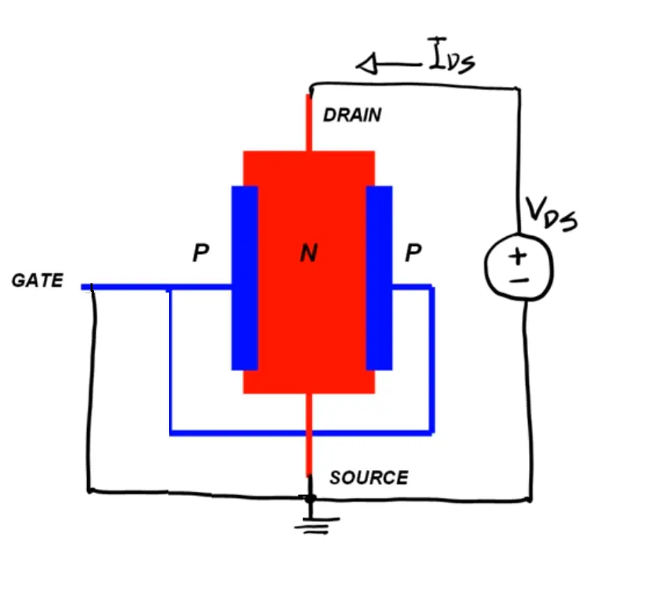
Now we connect a N channel JFET with an external source, such as positive terminal is connected to the source terminals and negative terminal is connected to the source and gate of the JFET and negative terminal will be grounded as shown in the figure. In this condition, drain region gets higher potential as compared with gate, hence junction between drain and gate will be reverse biased. Therefore, the depletion between these region will be thicker. Also the width of the depletion region is directly depending on the potential difference between drain and gate.
Ok Now You may get a doubt about why the depletion region nearer to the source terminal is thicker than the source region. Let see the answer,
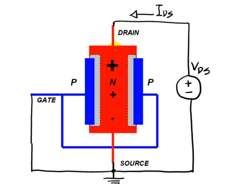
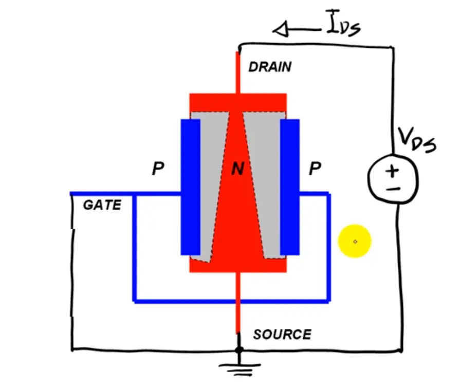
In Above diagram we applies higher potential at the drain terminal and lower potential at the source and source is grounded, therefore the higher potential region provides more voltage stress nearer to the junction, due to this reason the width of the depletion region is nearer to the drain is bigger than the source. Also due to this condition, the majority carriers (free electrons) flows from drain terminal to source terminal linearly. When We increases the potential difference between drain to source the current flows continuously. Even though for certain amount of increasing voltage VDS, the The JFET stops current flowing this voltage is called pinch-off voltage. The channel will be closed completely by the depletion layer. In this condition the JFET acts as voltage controlled resistor. At this condition, the drain current will be zero for theoretically, but a small amount of constant current will be flowing through the channel.
Ok Now You may get a doubt about why JFET allows a small amount of drain current when the channel is pinched off?
[wp_ad_camp_5]
Take an simple ohms law calculation V=R/I, Since current I= V/R, for Us ID=VDS/Rchannel Here you can observe that, as we said above when we increase the potential difference between drain to source, the width of the deletion region also increases, then channel resistance also increases proportionally, Therefore, dividing two proportional data we get constant result.
i.e
- consider V=5 Volts, R= 5 => I= 1
- consider V= 10 Volts, R= 10 ohms => I=2
Note: These data are only for understanding
Because of this phenomenon, the depletion layers never touch, and there would always be a narrow channel to facilitate the drain current to flow. Therefore, the drain current almost constant for the constant voltage VDS
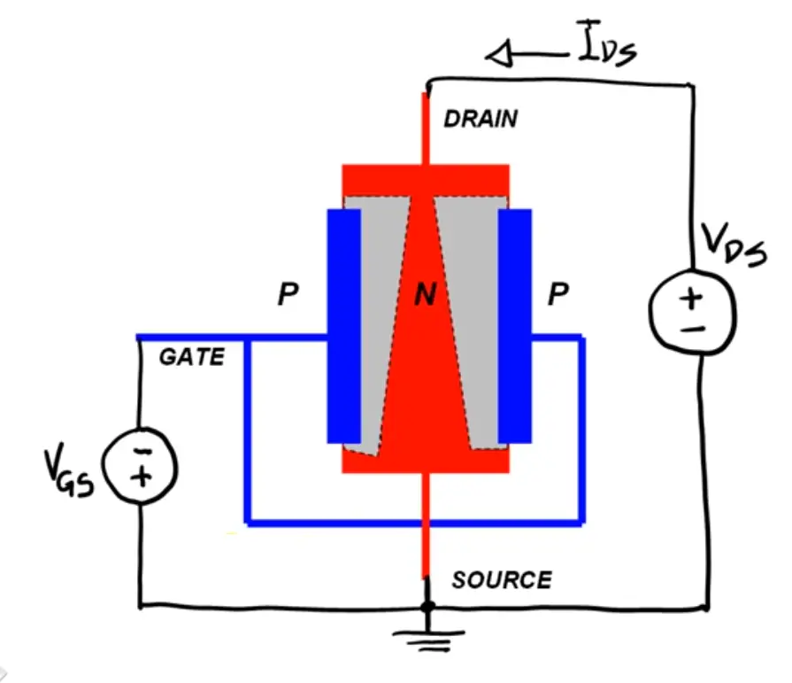
Also, Now we connect a negative voltage at the gate terminal, and we increase slowly which means 0 to -V voltages, the voltage difference between the channel and gate region increases hence the width of the depletion layer gets increased. Hence here also opening of the channel gets reduced which causes a decrease in drain current even at fixed drain voltage.
This is Working principle of N channel JFET (Junction Field Effect Transistor). If You Have Doubt, Then Feel free to comment us.
[wp_ad_camp_3]


